
MOSFET Semiconductor Technology Guide

Your Trusted Partner in Electronics Supply Chain. Inquire Now!

Explore Our Latest Smart Electronics Collection.

, , 
Inquiry
Inquiry

mosfet semiconductor

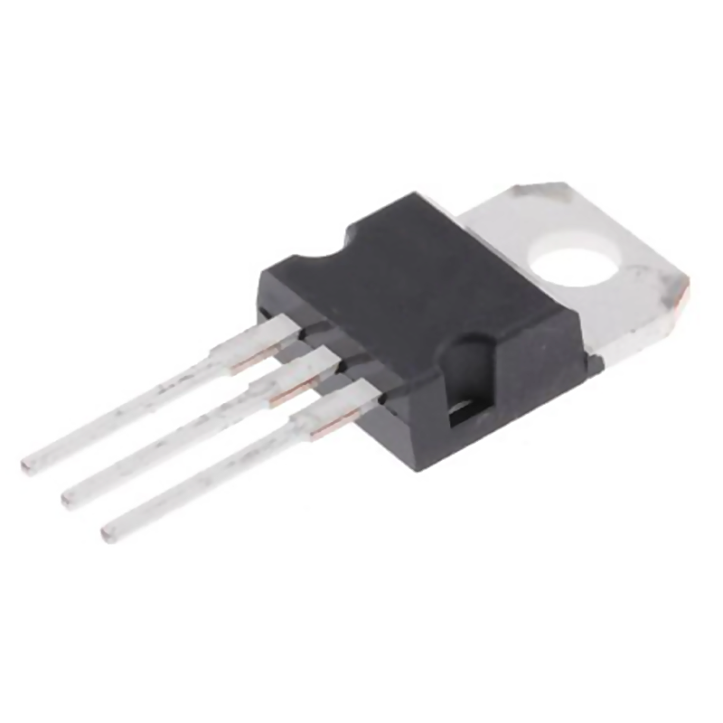
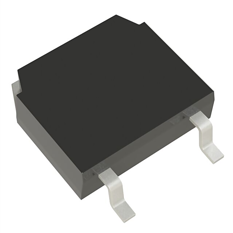
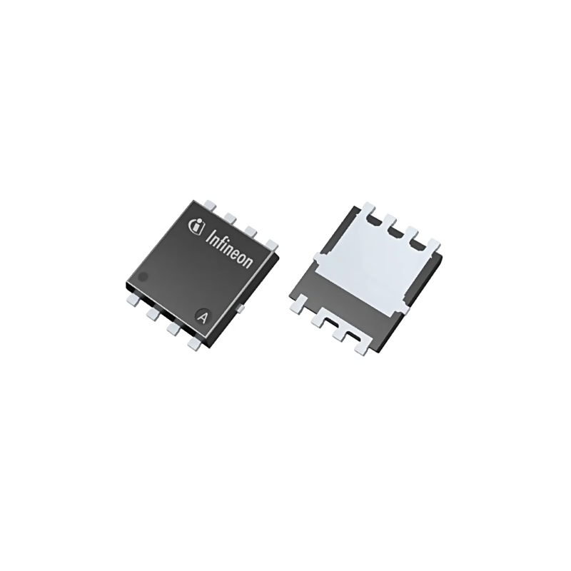
The mosfet semiconductor stands as a cornerstone component in modern electronic systems, serving as a voltage-controlled switch that enables precise control of electrical current flow. MOSFET, which stands for Metal-Oxide-Semiconductor Field-Effect Transistor, operates by applying voltage to its gate terminal to create an electric field that controls the conductivity between the drain and source terminals. This mosfet semiconductor technology has revolutionized power management and signal processing across countless applications. The device consists of three main terminals—gate, drain, and source—along with a substrate or body terminal. When voltage is applied to the gate, it creates a conductive channel that allows current to flow from drain to source, effectively acting as an electronically controlled switch. The mosfet semiconductor comes in two primary types: enhancement mode and depletion mode, with N-channel and P-channel variations available for each type. This versatility allows engineers to design circuits that meet specific performance requirements. Key technological features include high input impedance, fast switching speeds, low power consumption during operation, and excellent scalability for integration into compact designs. These characteristics make the mosfet semiconductor ideal for power supplies, motor controllers, audio amplifiers, digital logic circuits, and renewable energy systems. The technology continues evolving with improvements in breakdown voltage ratings, on-resistance values, and thermal performance, making the mosfet semiconductor increasingly efficient for demanding applications in automotive electronics, telecommunications infrastructure, consumer electronics, industrial automation, and renewable energy conversion systems.
Choosing a mosfet semiconductor delivers substantial practical benefits that directly impact your product performance and operational costs. First, these devices consume minimal power during static operation because the gate draws virtually no current, reducing energy waste and extending battery life in portable applications. This efficiency translates to lower electricity bills in industrial settings and longer runtime for battery-powered devices. Second, the mosfet semiconductor switches extremely fast, often in nanoseconds, enabling high-frequency operation that improves system responsiveness and reduces switching losses. This speed advantage makes your equipment more efficient and capable of handling demanding real-time processing tasks. Third, the high input impedance of the mosfet semiconductor means it places minimal load on preceding circuit stages, simplifying driver circuit design and reducing component count, which lowers manufacturing costs and improves reliability. Fourth, these devices operate at lower temperatures compared to alternative technologies, reducing cooling requirements and improving system longevity. This thermal advantage means fewer failures, lower maintenance costs, and improved safety margins in your applications. Fifth, the mosfet semiconductor offers excellent scalability, allowing manufacturers to integrate millions of these devices onto single chips for complex digital systems or use individual units for high-power applications. This flexibility ensures you can select the right solution regardless of your power handling needs. Sixth, modern mosfet semiconductor devices feature robust construction with high reliability ratings, often exceeding millions of switching cycles without degradation. This durability ensures your products maintain consistent performance throughout their service life, reducing warranty claims and enhancing customer satisfaction. Finally, the widespread availability and competitive pricing of mosfet semiconductor technology make it a cost-effective solution that delivers professional-grade performance without premium pricing, helping you maintain competitive product pricing while delivering superior functionality.

Tips And Tricks

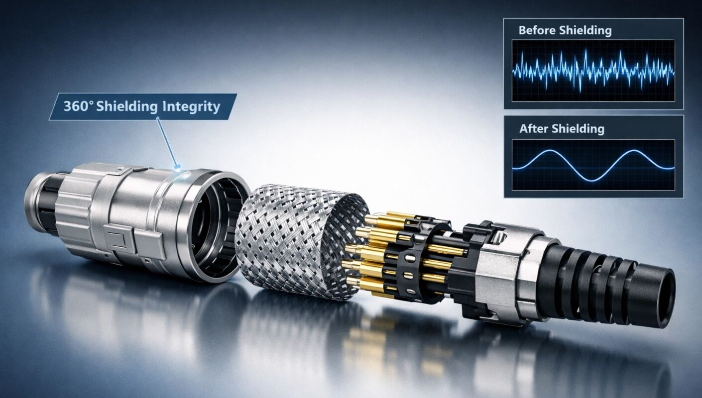
Why Shielded Connectors are Critical for Industrial Robotics: Overcoming EMI in High-Speed Automation

11

May

Why Shielded Connectors are Critical for Industrial Robotics: Overcoming EMI in High-Speed Automation

Struggling with robotic jitter, ghost failures, or positional drift? Shielded connectors eliminate EMI in high-speed automation—boost uptime & precision. Get the engineering guide.
View More
How does a mosfet transistor improve efficiency in industrial power systems?

12

Jun

How does a mosfet transistor improve efficiency in industrial power systems?

View More
Why do engineers choose mosfet transistor devices for power management designs?

12

Jun

Why do engineers choose mosfet transistor devices for power management designs?

View More
Is a power management ic essential for efficient energy regulation in devices?

12

Jun

Is a power management ic essential for efficient energy regulation in devices?

View More
Superior Energy Efficiency and Thermal Performance

Superior Energy Efficiency and Thermal Performance

The mosfet semiconductor excels in energy efficiency through its unique voltage-controlled operation mechanism that eliminates the need for continuous gate current. Unlike current-controlled devices, the mosfet semiconductor maintains its conductive state with only a voltage potential at the gate, drawing virtually zero steady-state current. This fundamental advantage dramatically reduces power dissipation, particularly in applications requiring prolonged on-states. The efficiency gains become especially significant in battery-operated devices where every milliwatt of saved power extends operational time. Additionally, the mosfet semiconductor generates less heat during operation due to lower conduction losses and faster switching transitions that minimize time spent in the high-dissipation linear region. This superior thermal performance reduces stress on the component and surrounding circuitry, extending overall system lifespan. Lower operating temperatures also decrease the need for expensive heat sinks and cooling systems, reducing both initial costs and ongoing energy consumption for active cooling. For designers, this thermal advantage provides greater flexibility in compact designs where space for cooling solutions is limited, enabling smaller, lighter products without compromising reliability or performance specifications.
Ultra-Fast Switching Capabilities for Modern Applications

Ultra-Fast Switching Capabilities for Modern Applications

The mosfet semiconductor delivers exceptional switching speed that proves essential for contemporary high-frequency applications ranging from switch-mode power supplies to radio-frequency systems. With switching times often measured in nanoseconds, the mosfet semiconductor enables operation at frequencies extending into the megahertz range, far exceeding capabilities of older transistor technologies. This rapid switching capability directly translates to improved system performance through reduced switching losses, higher operational frequencies, and better signal fidelity. In power conversion applications, faster switching allows designers to use smaller inductors and capacitors, significantly reducing system size and weight while maintaining or improving efficiency. The quick response time of the mosfet semiconductor also enables precise pulse-width modulation control for motor drives and LED dimming, providing smooth, flicker-free operation with fine resolution. For digital circuits, the fast switching characteristics support higher clock speeds and greater computational throughput. Furthermore, the reduced transition time minimizes electromagnetic interference generation, helping products meet stringent regulatory requirements. This combination of speed and clean switching makes the mosfet semiconductor the preferred choice for designers seeking to maximize performance while minimizing size, cost, and electromagnetic compatibility challenges in their electronic systems.
Exceptional Scalability Across Power Ranges

Exceptional Scalability Across Power Ranges

The mosfet semiconductor demonstrates remarkable versatility through its ability to scale effectively from milliwatt signal processing applications to megawatt power conversion systems, providing consistent operating principles across this vast power spectrum. This scalability stems from the fundamental physics of the mosfet semiconductor design, which can be optimized for specific voltage and current requirements by adjusting channel dimensions, doping concentrations, and geometry. For low-power digital applications, manufacturers produce mosfet semiconductor devices with minimal die area, enabling billions of transistors on single integrated circuits that power smartphones, computers, and IoT devices. At the opposite extreme, power mosfet semiconductor variants handle hundreds of amperes and thousands of volts for industrial motor drives, electric vehicle inverters, and grid-tied renewable energy systems. This range flexibility allows engineers to standardize on mosfet semiconductor technology across product lines, leveraging familiar design methodologies and reducing learning curves. The consistent voltage-controlled operating principle simplifies driver circuit design regardless of power level, with differences primarily in gate charge requirements rather than fundamental control strategies. This universality accelerates development timelines and reduces engineering costs while ensuring reliable performance across diverse applications, making the mosfet semiconductor a truly universal solution for electronic switching and amplification needs.